


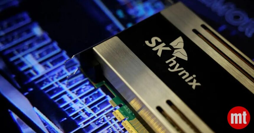
SK Hynix just broke ground on a $4 billion AI chip packaging plant in Indiana, marking one of the largest semiconductor investments on U.S. soil. The facility sits inside the Purdue Research Park in West Lafayette. Cleanroom operations are scheduled to begin in the second half of 2028.
In This Article
Key Highlights
- SK Hynix commits $4 billion to a West Lafayette, Indiana AI chip packaging facility
- Cleanroom operations targeted for second half of 2028 at Purdue Research Park
- Site will include a next-generation HBM packaging line and an AI semiconductor R&D center
SK Hynix Launches $4 Billion AI Chip Packaging Facility in Indiana
SK Hynix held the official groundbreaking ceremony for its AI chip packaging plant in West Lafayette, Indiana, confirming a $4 billion capital commitment. The Purdue Research Park site will house a high-bandwidth memory packaging line built to serve surging global demand from AI data center operators. India-based suppliers and semiconductor firms watching U.S. fab investments are paying close attention, as this reshapes where advanced AI memory gets produced and tested at scale.
HBM Production and the Global Impact of AI Chip Packaging
The West Lafayette plant will run a dedicated AI chip packaging line for next-generation high-bandwidth memory, the exact memory type powering Nvidia GPU clusters and similar AI accelerators. SK Hynix already leads global HBM supply, shipping stacked memory to the world’s largest AI hardware buyers. Adding domestic U.S. capacity tightens SK Hynix’s grip on the HBM supply chain while reducing geopolitical exposure risks that have rattled chipmakers since 2026 export controls took hold.
“SK Hynix placing AI chip packaging capacity inside the United States directly responds to customer pressure from hyperscalers who want supply chain security close to home. This is a calculated move to protect long-term HBM contracts.” — Industry Analyst, Telecom Sector
What Happens Next
SK Hynix will advance construction through 2026 and 2027 before cleanroom equipment installation begins. The company targets full AI chip packaging operations in the second half of 2028. The attached R&D center will run concurrent to production, accelerating next-generation HBM development. Global telecom and AI hardware suppliers, including Indian firms building AI inference infrastructure, should monitor procurement windows opening as the Indiana facility ramps toward commercial output.
Sources: GSMA ↗ | COAI ↗ Economic Times, SK Hynix official press statements
People Also Ask
- Where is SK Hynix building its new AI chip packaging facility? SK Hynix is building the facility at Purdue Research Park in West Lafayette, Indiana. The $4 billion site includes an HBM packaging line and an AI semiconductor R&D center.
- When will the SK Hynix Indiana plant start operations? Cleanroom operations are scheduled to begin in the second half of 2028, according to SK Hynix’s official press statements and website disclosures.
- What type of chips will SK Hynix produce in Indiana? The Indiana plant will package next-generation high-bandwidth memory chips, the same HBM technology used in AI accelerators from companies like Nvidia.